Mistakes are the portals of discovery.
- James Joyce
Growing up is not easy. Take nanowires: With no support or guidance, they become unruly, making it difficult to harness their full potential. Prof.
Ernesto Joselevich of the Weizmann Institute’s Chemistry Faculty has found a way to grow nanowires out – not up – providing the support and guidance they need to become long, orderly aligned structures. Since semiconductors with controlled structures are at the core of the most advanced technologies, this new research will hopefully enable the production of semiconductor nanostructures with enhanced electronic and optical properties with a wide range of applications, among them transistors, LEDs, lasers, information storage media computers and photovoltaics.
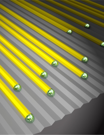
Most nanowires actually start out with a successful “upbringing”: In the so-called vapor-liquid-solid (VLS) technique, vaporized raw semiconductor materials are dissolved in a tiny metal droplet placed on a surface. The semiconducting nanowire grows upward – a bit like a stalagmite – as the material crystallizes and more is deposited. Such wires are defect-free and exhibit excellent optical and electronic properties, as their lack of contact with the surface allows them to grow up in a stress-free environment. The problems show up later, when it is time to harvest the nanowires and assemble them into structured arrays. Then, the fragile nanowires often break into little pieces, get entangled and resist alignment – limiting their use in many applications. But horizontal growth, which might yield stronger nanowires, also has its shortcomings: The underlying surface usually introduces stress, causing defects and leading to subpar optical and electronic properties in the semiconductor material.
Joselevich and his team’s first hint that these shortcomings might be surmountable came in earlier research, when they discovered that growing carbon nanotubes on sapphire that had mistakenly been cut a few degrees off from the main crystal plane mysteriously resulted in the growth of well-aligned, millimeter-long nanotubes. Upon closer inspection, they found that the uneven cut had created “steps” of atomic dimensions between the crystal’s planes, guiding the growth of the nanotubes into orderly, well-aligned arrays.
In their new research, Joselevich, together with Ph.D. student David Tsivion and postdoctoral fellow Dr. Mark Schvartzman of the Materials and Interfaces Department, took this technique a step further and for the first time used sapphire steps to try to control the horizontal growth of nanowires. This time, they deliberately cut the sapphire along different planes of the crystal, resulting in a variety of surface patterns: smooth, step-like and accordion-like (V-shaped) grooves. They then used the VLS method to grow nanowires of gallium nitride (GaN) – a popular semiconducting material that is the basis of the blue LEDs used in outdoor TV screens and the violet lasers used in Blu-ray discs.
Their results, which appeared in
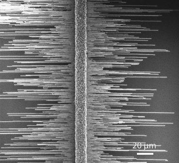
Science, show that, unlike smooth surfaces, steps and grooves have a strong guiding effect: The nanowires grow horizontally along the edges of and within the grooves into well-aligned, millimeter-long structures. The scientists found that they could even control the orientation of the atoms within the nanowire by altering the direction of the sapphire cut. This orientation is known to affect the nanowires’ properties, and it could be relevant to photonic, optoelectronic and radio frequency applications.
The scientists were pleased to find that their nanowires’ electrical and optical properties were just as good as – if not better than – those of vertically-grown nanowires. Joselevich: “This was very surprising, as we expected to see at least some degradation in quality due to contact with the surface.”
Although it is still not clear exactly how the VLS method produces horizontal nanowires, Joselevich and his team have managed to combine, in a single step, the synthesis and assembly of well-structured nanowires with unique properties suitable for a wide range of applications, simply by getting them “into the groove.”
Edible nanowires
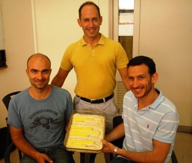
Having a paper accepted to Science is cause for celebration. To let his students in on the good news, Joselevich summoned them to an “urgent meeting,” where he surprised them with cake and champagne. The orange sponge cake was baked by his wife, but Joselevich supplied the decoration: He sliced grooves into the cake’s surface and frosted it with white chocolate, topping the grooves with “nanowires” in yellow icing and silver sugared almonds representing the wires’ nanoparticle catalyst.
Prof. Ernesto Joselevich’s research is supported by the Carolito Stiftung.


