Are you a journalist? Please sign up here for our press releases
Subscribe to our monthly newsletter:
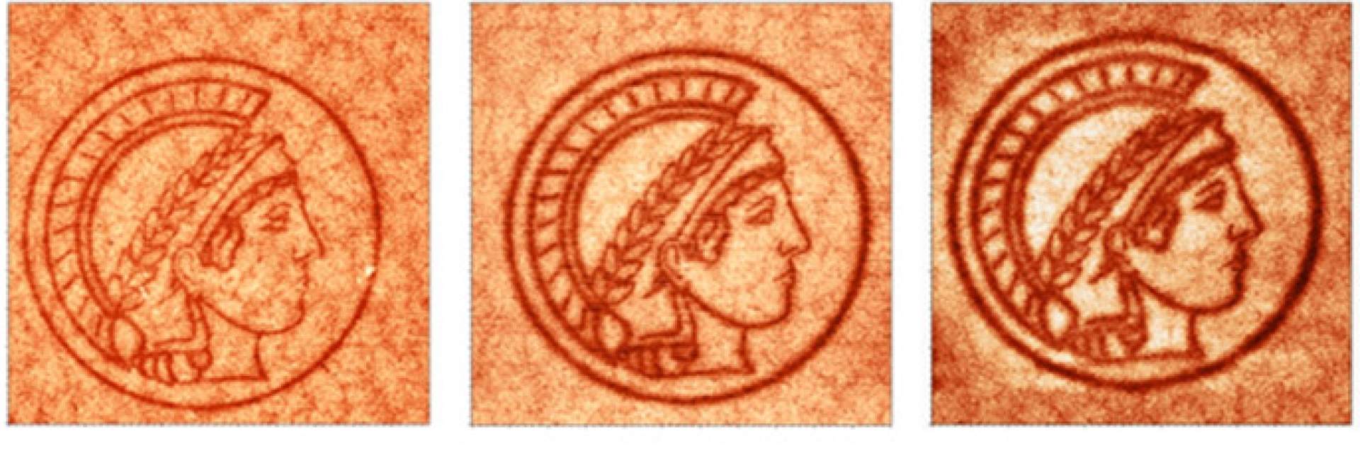
 in diameter, made of nanodot sequences “written” with a narrow electron beam on the surface of a self-assembled monolayer. The strength of the chemical transformation in the monolayer increased with the duration of each nanodot’s exposure to the beam – from 10.8 microseconds (left) to 32.4 (center) to 48.6 (right). Viewed with an atomic force microscope")
Short of shrinking ourselves to the size of molecules or atoms, how can we fully benefit from the emerging wonderland of nanoscale devices? These tiny devices promise one day to provide vast data storage capacity and a host of other exciting possibilities; but effectively incorporating them into our macro-sized world remains a huge challenge. A new methodology for creating patterns on the nanoscale, developed at the Weizmann Institute of Science, may help bridge the million-fold gap in size between the worlds of nano and macro.
The trigger for this project had been a surprising observation in the laboratory of Prof. Jacob Sagiv of the Department of Materials and Interfaces. Staff scientist Dr. Rivka Maoz had exposed an ultrathin layer of an oxygen-containing polymer deposited on a self-assembled monolayer – a one-molecule-thick layer of a soap-like material adsorbed on silicon – to a beam of electrons of the kind that is often used to create nanostructures by a technique known as electron beam lithography. Normally, this polymer is easily peeled off from the monolayer, but following the exposure to the electron beam, the two materials remained firmly glued together. After investigating this unexpected finding, the scientists concluded that the electron beam induces a lasting chemical change in the top surface of the monolayer, as the result of an oxidation reaction with oxygen released at the boundary between the polymer and the monolayer.
 Drs. Doron Burshtain and Ora Bitton, Prof. Jacob Sagiv and Dr. Rivka Maoz")
As reported recently in ACS Nano, the research team – which included also Dr. Jonathan Berson, Dr. Doron Burshtain, Dr. Peter Nelson and Ariel Zinger, all of the Department of Materials and Interfaces, and Dr. Ora Bitton of the Chemical Research Support Department – built on this discovery to develop a method for creating nanoscale chemical patterns. The method consists of inducing chemical modifications with the help of a narrow electron beam directed to preselected surface sites. In this manner, it is possible to modify only those sites deliberately exposed to the electron beam, while no chemical changes occur in unexposed regions of the monolayer.
By controlling where exactly the beam is applied, the researchers managed to create elaborate patterns of chemically modified regions on the monolayer surface. The patterns were visualized by atomic force microscopy, which can capture chemical differences between modified and unaltered surface regions.
The researchers later showed that not only a polymer film, but also other ultrathin films – including metal ones – could be used as catalysts to generate chemical transformations induced by electron beams, and that such transformations occurred on a variety of surfaces. In other words, the study’s findings have a generic value: They advance a new chemical approach to surface patterning.
The nondestructive chemical approach produces seamless surface patterns devoid of defects
This new chemical patterning methodology could serve to create nanoscale patterns for numerous purposes. For example, it may be used to create new types of single-layer electronic circuits – by alternating surface regions that conduct an electric current with those that do not.
Inducing local chemical reactions that modify only the outer atomic layer of a material in selected regions, without affecting neighboring surface regions or the bulk of the material underneath, represents a radically new approach to creating nanopatterns – one that offers unique advantages. Existing methods employing electron beams to create nanopatterns rely either on destructive processes, such as “digging” into the material, or, conversely, on the addition of a different material in selected surface regions. In both cases, structural defects at the boundaries of patterned features are practically inevitable. In contrast, the present, nondestructive chemical approach produces seamless surface patterns devoid of defects, a major plus in many applications – and a particularly critical one in electronic circuits.
No less important, other methods for producing nanopatterns operate on the nanoscale only, which means that additional technologies are required to connect the nanodevices to the macro world. Such connections are challenging to build and can easily become a source of malfunction. The chemical approach can solve this problem by creating patterns that span the full range of dimensions from nano to macro. Thus the researchers are currently investigating electrically conducting “channels” produced by the patterning of atomically thin surface strips measuring less than 20 nanometers (millionths of a millimeter) in width but over 20 millimeters (2 centimeters) in length – equivalent to a highway 20 meters wide and 20,000 kilometers long, that is, spanning half of the circumference of Earth. This means that nanodevices created by the chemical method could be directly suitable for real-world use, with no need for in-between technologies.