Are you a journalist? Please sign up here for our press releases
Subscribe to our monthly newsletter:

The lens in the camera or microscope of the future might be “printed” on an advanced version of a 3-D printer; and it could be much thinner and more accurate than those found today. Research conducted jointly at the Weizmann Institute of Science and Tel Aviv University, which was recently published in Nature Communications, describes ultrathin lenses that are comprised of nanomaterials and designed with extreme precision. These lenses, which contain several distinct nanolayers, could alleviate the current need for multi-element lenses – replacing them with a single, thin optical device.
For hundreds of years, people have controlled the functions of lenses by controlling the thickness and curvature of the material, later improving the resulting images by combining a number of lenses into a single optical element. In the lab of Prof. Yehiam Prior in the Weizmann Institute’s Chemical Physics Department, such optical elements as lenses are not curved, but rather make use of metasurfaces – materials containing nanostructures that modify one or more of the properties of light waves. These are designed with computer algorithms and are precisely fabricated to nanoscale resolutions. By altering the composition, shape, angle and position of these nanostructures, the scientists in his group have learned how to bend and shape light waves to exacting specifications.
Even a cell phone will have around seven (lenses). Otherwise, your images will be a mess
With metasurfaces, explains Prior, one can tinker with the different parameters of light. “When lenses modify the properties of light waves, they alter one that is rarely talked about – the phase, or timing, of the waves. In standard optical lenses a displacement known as chromatic aberration arises because the phases of different light waves are unequally delayed.”
With chromatic aberrations, the lens alters the phase differently for different colors, and as a result the focal point for blue – the shorter waves – is offset from that of red – the longer waves. (Prisms and rainbows work on much the same principle.) In order to compensate for this aberration, lenses in even the simplest device are made up of several different elements, each with a slightly different focus so as to correct the displacement of one color in the image. “You can have up to 13 of these elements in a microscope or projector. Even a cell phone will have around seven. Otherwise, your images will be a mess,” says Prior.

Prior and postdoctoral fellow Dr. Euclides Almeida realized that the metasurfaces they worked with might be used to create a single, chromatically corrected lens. They began their quest by asking how to approach the issue of color: Visible light can be divided into thousands of wavelengths, but the receptors in our eyes are primed to see just three – red, green and blue (or RGB, as it is generally known). RGB is the basis of all electronic imagery: Pixels add the three together in various proportions to re-create the illusion of a full color spectrum.
The scientists thus decided on lenses of three layers, each containing a metal that was most suited to focusing one particular wavelength of light – gold for red, silver for green and aluminum for blue. Together with Prof. Tal Ellenbogen and Ori Avayu of Tel Aviv University, they worked out the best way to arrange and fabricate arrays of thousands of nanoscale metallic disks in successive thin films of silicon – each layer designed separately.
The multilayered lenses were produced with electron beam lithography technology in the clean room of the Weizmann Institute’s Chemical Research Support Department, with the expert assistance of Dr. Ora Biton. The group eventually managed to get the relative accuracy of their three layers to under 10 nanometers, an unusual achievement that might lead to applications in which very high resolution is required.
“Learning how to print the lens in layers was not trivial,” says Prior. “But once we managed to optimize our materials for each color and understand how to design our layers, getting the focal points of each layer to align properly was the easy part. We can now use what we have learned about optimization to control other optical elements.”
One especially exciting possible future application of this technology might be in high-resolution microscopy, particularly in a technique known as STimulated Emission Depletion microscopy, or STED. The technique, which garnered its inventor a Nobel Prize in 2014, was created to overcome a limitation of conventional light microscopy – you can’t focus light to a spot that is smaller than the wavelength of light, about one micron. STED, explains Prior, “makes use of a very nice optical trick. Typically, you excite all of your sample with one colored laser, so that it fluoresces – i.e. it gives back some light. Next you cancel some of that light with a second colored laser – for example, one that forms a donut shape around the part you want to see – and then you ‘tighten’ this blocking donut further till the desired resolution is achieved.”

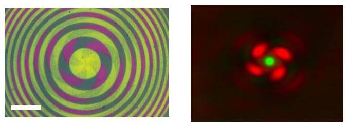
The researchers surmised that layered lenses might make this process more accessible: “We found that we could generate the light distribution so that two colors do two different things. As an example, we demonstrated the concept with an image of a green spot inside a red donut,” says Prior.
“Today, STED microscopy entails an entire lab-sized optical table,” adds Almeida. “In the future, this setup might be replaced by a single, micron-thick lens. Of course, our research is just a preliminary step in that direction.”
“Although the technique is a bit complex, it works, in principle, something like 3-D printing, which produces objects layer by layer,” says Prior. “Even now, we design lenses or other optical elements on our computers with algorithms that are sophisticated versions of those for 3-D printing, and then we go down to the clean room to make them. Our accuracy, as well as the things we manage to do with these lenses, can only improve.”
Prof. Yehiam Prior's research is supported by the Mary and Tom Beck-Canadian Center for Alternative Energy Research; the Leona M. and Harry B. Helmsley Charitable Trust; and Dana and Yossie Hollander, Israel. Prof. Prior is the incumbent of the Sherman Professorial Chair of Physical Chemistry.