Are you a journalist? Please sign up here for our press releases
Subscribe to our monthly newsletter:

This it is the story of a unique material – made of a single compound, it conducts electrons in different ways on its different surfaces and doesn’t conduct at all in its middle. It is also the story of three research groups – two at the Weizmann Institute of Science and one in Germany, and the unique bond that has formed between them.
The material belongs to a group of materials discovered a decade and a half ago known as topological insulators. These materials are conducting on their surfaces and insulating in their inside “bulk.” But the two properties are inseparable: Cut the material, and the new surface will be conducting, the bulk will remain insulating.
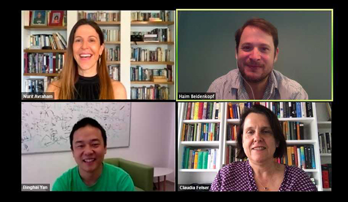
Some five years ago, Dr. Nurit Avraham was a staff scientist in the new group of Dr. Haim Beidenkopf of the Institute’s Condensed Matter Physics Department. Around that time, she and Beidenkopf met Prof. Binghai Yan on Yan’s first scientific visit to the Weizmann Institute. Back then Yan was working as a junior group leader within the group of Prof. Claudia Felser, a materials scientist who was developing new kinds of topological materials in her lab at the Max Planck Institute for Chemical Physics of Solids in Dresden. Beidenkopf and his group specialize in classifying and measuring these materials on the scale of single atoms and the paths of single electrons, while Yan was turning to theory – predicting how these materials should behave and working out the mathematical models that explain their unusual behavior.
Avraham and Beidenkopf were interested in uncovering the properties of a special type of topological insulator in which the chemical structure is organized in layers. How would the layers affect the way that electrons were conducted over the surface of the material? Theoretically, stacking layers of 2D topological insulator was expected to form a 3D topological insulator in which some of the surfaces would be conducting and some insulating. Yan suggested they work with a new material being predicted by him and later developed in Felser’s lab. Soon the Weizmann and Max Planck groups started collaborating.

Avraham led the project, obtaining samples of the material from Felser’s lab, guiding the measurements, and working with Yan to see whether the theories’ predictions would be borne out experimentally. As the collaboration deepened, Beidenkopf and Avraham got the Faculty of Physics to again invite Yan to the Institute, and this visit eventually led Yan to decide to leave Germany and move his family to Rehovot, to take up a position in the Institute’s Condensed Matter Physics Department. “That decision was a turning point that would set me on my present career path,” says Yan.
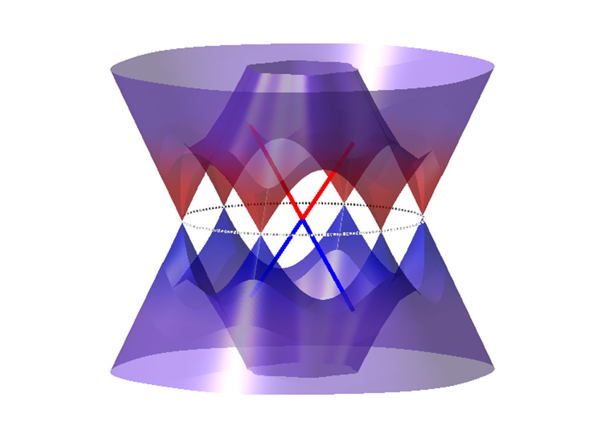
Over the coming years, Beidenkopf, Avraham, Yan and Felser would collaborate on multiple research projects, exploring the properties of several different classes of topological materials. But understanding this particular material – a compound of bismuth, tellurium and iodine – would turn out to be a long-term project. To begin with, Yan analyzed the band structure of the material – in other words, the states electrons are “allowed” to inhabit. When the bands get crossed in the bulk – so called “band inversion” – they prevent electrons from moving around inside, but enable them to move on the surface. This “projection” of a state arising in the bulk of a material onto the surface is what gives topological materials their special properties.
Avraham and Beidenkopf worked with samples that had been cleaved, exposing fresh surfaces out of the layered structure. They used a scanning tunneling microscope – STM – in their lab to track the electron density in the different parts of the material. The theory predicted that the surface measurements would reveal a material that behaves as a weak topological insulator, thus being metallic on the edges and insulating on the top and bottom surfaces. Weak topological insulators were a class of topological materials that had been predicted but not yet proven experimentally, so the group was hoping to uncover such characteristic properties on the edges’ surfaces. The researchers did, indeed, find that the material acted as a weak topological insulator on its cleft sides. But on the tops and bottoms of their samples, the group found evidence indicating a strong topological insulator, rather than the weak insulator that had been predicted.
As the collaboration deepened, Beidenkopf and Avraham got the Faculty of Physics to again invite Yan to the Institute
Could this one material be not only at the same time insulating and conducting, but conduct in two different ways? As the researchers continued to experiment, testing the material with different methods and confirming their original results, together with Yan they continued to puzzle over the strange results. At one point, says Avraham, they even measured a new batch of samples that were grown independently by junior Prof. Anna Isaeva and Dr. Alexander Zeugner at the Technische Universit ̈at Dresden, just to be sure the results were general and not an accidental property of one particular batch of samples.
Part of their eventual breakthrough says Yan, came from a theoretical research paper published by another physics group that conjectured how such a dual material might function. Topological materials are sometimes classified according to their symmetry – a property of the atomic structure of the material. The scientists looked for places on the surfaces where any such symmetry would be broken, due to flaws or irregularities on the surface, which, by scattering electrons, would affect the properties in that spot and highlight the type of symmetry “protecting” each topological state.
Finally, theory and experiment came together to show, in an article published in Nature Materials, that the material is, indeed, two different kinds of topological insulator in one. The exposed layers of the cleft, side surfaces create “step-edges” that channel the electrons into certain paths. While the sides are protected by both time reversal and translational symmetry, the tops and bottoms are protected by crystalline mirror symmetry, giving rise to a metal-like state in which the electrons can move.
While this two-in-one combination made it challenging to classify the material topologically – one of the main goals of such measurements – the researchers believe that other new topological materials could turn out to have such dual properties. That opens the possibility of engineering materials to have several desired electrical properties all in one.
“Technically, the work was challenging, but the story, itself, turned out to be simple,” says Yan.
“It’s also the story of a great friendship and what happens when you can have such close scientific collaboration,” says Avraham.
“And it all started with a question about a particular kind of material,” adds Beidenkopf.
Dr. Haim Beidenkopf's research is supported by the Leona M. and Harry B. Helmsley Charitable Trust. Dr. Beidenkopf is the incumbent of the Recanati Career Development Chair of Energy Research in Perpetuity.
Prof. Binghai Yan's research is supported by the Willner Family Leadership Institute; and the European Research Council.